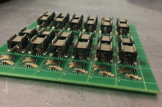
Circuit Card Assembly: The Key to Advanced Manufacturing

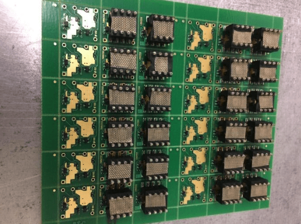
Introduction

Circuit card assembly (CCA) is a crucial component in the manufacturing process for numerous industries, including aerospace, energy, and startup technology companies. As these sectors strive to develop new products, the demand for quick-turnaround, high-quality printed circuit board (PCB) assembly services has never been higher. 

The New Product Introduction (NPI) processes, prototyping, testing, and validating new designs all rely heavily on efficient and precise circuit card assembly. This blog explores the importance of CCA, the challenges faced by companies in these industries, and the solutions available to meet their needs.

The Significance of Circuit Card Assembly

Circuit card assembly involves mounting electronic components onto a PCB, which serves as the foundation for most electronic devices. This process is critical in transforming a simple board into a functional circuit, capable of performing complex tasks. For industries like aerospace and energy, the reliability and performance of these assemblies are paramount, as they directly impact the safety and efficiency of the final products.

In aerospace, circuit card assemblies are used in navigation systems, communication devices, and control mechanisms. The energy sector utilizes CCAs in monitoring systems, control panels, and smart grid technologies. Startups and technology companies rely on these assemblies to bring innovative products to market, making the role of these types of assembly pivotal across these diverse fields.

Challenges

Demand for Quick Turnaround: Circuit Card Assembly

The rapid pace of technological advancement requires companies to move swiftly from concept to market. Quick-turnaround times are essential to stay competitive, particularly for startups looking to capitalize on new opportunities.

High-Quality Standards:

A good quality policy is non-negotiable in industries like aerospace and energy, where the smallest defect can lead to significant safety hazards or operational failures. Ensuring high standards in CCA is crucial for the credibility and success of these companies.

Complexity of Designs: Circuit Card Assembly

Modern electronic devices are becoming increasingly complex, requiring intricate circuit designs and precise assembly techniques. This complexity can pose significant challenges in the production process.

Cost Management:

Balancing cost with quality and speed is a constant challenge. Companies need to optimize their processes to maintain affordability while ensuring top-notch quality and rapid delivery.

Solutions for Efficient Circuit Card Assembly

To address these challenges, companies must adopt advanced manufacturing techniques and collaborate with experienced PCB assembly service providers. Here are some key strategies:

Leveraging Advanced Technologies:

Utilizing cutting-edge technologies such as automated optical inspection (AOI), X-ray inspection, and robotic assembly can significantly enhance the accuracy and efficiency of the CCA process. These technologies help in detecting defects early, ensuring high quality and reducing rework costs.

Partnering with Reliable Suppliers:

Establishing partnerships with reputable PCB assembly service providers can ensure access to high-quality components and expertise. These suppliers can offer valuable insights and support throughout the NPI process, from prototyping to final production.

Implementing Agile Manufacturing Processes:

Agile manufacturing techniques, including just-in-time (JIT) production and lean manufacturing principles, can streamline the assembly process, reducing lead times and costs. These approaches focus on eliminating waste and improving efficiency.

Investing in Skilled Workforce:

A skilled workforce is essential for managing the complexities of modern CCA. Continuous training and development programs can equip employees with the necessary skills to handle advanced assembly techniques and technologies.

Prototyping and Testing: Circuit Card Assembly

Early prototyping and rigorous testing are crucial for validating new designs. By identifying potential issues during the prototyping phase, companies can make necessary adjustments before moving to full-scale production, saving time and resources.

Circuit Card Assembly: Case Studies

Aerospace Innovations: 

An aerospace company may partner with an advanced PCB assembly provider to develop navigation systems for next-generation aircraft. By leveraging automated assembly technologies and rigorous testing protocols, they can achieve reductions in production time while maintaining exceptional quality standards.

Energy Sector Advancements: 

An energy startup focused on smart grid technologies may utilize quick-turnaround PCB assembly services to prototype and test new monitoring systems. The collaboration should allow them to rapidly iterate on their designs, resulting in a market-ready product in a reasonable time frame. 

Startup Technology Breakthroughs: 

A tech startup developing wearable health devices may face challenges with miniaturization and complex circuitry. By partnering with a specialized PCB assembly firm, they can successfully prototype their device, conduct extensive testing, and launch their product, gaining a competitive edge in the market.

Circuit Card Assembly: Conclusion

This type of assembly plays an indispensable role in the advancement of technology across various industries. The demand for quick-turnaround, high-quality PCB assembly services is driven by the need for rapid innovation, especially in aerospace, energy, and startup technology sectors.

Overcoming the challenges of complexity, cost management, and quality assurance requires a combination of advanced technologies, strategic partnerships, agile manufacturing processes, and a skilled workforce.

As companies continue to push the boundaries of innovation, the importance of efficient and reliable circuit card assembly will only grow. By adopting the right strategies and leveraging the expertise of experienced assembly providers, businesses can navigate the complexities of the modern manufacturing landscape and achieve their goals of delivering cutting-edge products to the market.

Discover how partnering with an expert PCB assembly provider can enhance your product’s reliability and speed to market. Contact us today at Tracer to request a quote!

High Speed PCB: The Value of Assembly Support Activities

Introduction to High Speed PCB

The rapid evolution of technology and the increasing demand for sophisticated electronic devices have significantly impacted the manufacturing processes of high-speed printed circuit boards (PCBs). High speed PCBs are critical components in a wide range of applications, including telecommunications, aerospace, automotive, and industrial automation. 

These PCBs must meet stringent performance standards to ensure the reliability and efficiency of the final products. However, achieving these standards requires a comprehensive approach that includes several assembly support activities. 

This blog explores the importance of component sourcing, rework and repair, functional testing, X-ray inspection, encapsulation/potting/coatings, electro-mechanical assembly, and order fulfillment in the high speed PCB manufacturing process.

High Speed PCB: Component Sourcing

Component sourcing is a crucial step in the high speed PCB manufacturing process. The quality and compatibility of components directly influence the performance and reliability of the final product. 

Manufacturers must source components from reputable suppliers to ensure they meet the required specifications and standards. Additionally, the components must be compatible with the high speed PCB design to avoid performance issues such as signal interference and crosstalk.

Effective component sourcing involves:

Supplier evaluation:

Assessing suppliers based on their track record, quality certifications, and ability to deliver components on time.

Component verification: 

Conducting thorough inspections and tests to verify the authenticity and quality of the components.

Supply chain management: 

Maintaining a robust supply chain to mitigate the risk of component shortages and delays.

By prioritizing quality and compatibility during the component sourcing phase, manufacturers can enhance the overall performance and reliability of these components.

Rework and Repair

Despite the best efforts to ensure quality during the manufacturing process, defects can still occur. Rework and repair activities are essential to address these defects and improve the yield of high speed PCB components. These activities involve identifying and correcting issues such as soldering defects, misaligned components, and damaged traces.

Key aspects of rework and repair include:

Advanced repair techniques:

Utilizing state-of-the-art tools and techniques to repair defects without compromising the integrity of the PCB.

Skilled technicians:

Employing experienced technicians who are proficient in diagnosing and repairing high speed PCBs.

Quality control:

Implementing rigorous quality control measures to ensure repaired PCBs meet the required performance standards.

By effectively addressing defects through rework and repair, manufacturers can reduce waste, improve yield, and ensure the reliability of high speed PCBs.

Functional Testing

Functional testing is a critical step in the high speed PCB manufacturing process. This involves verifying that the PCB performs as intended under various conditions. Functional tests can include electrical performance tests, environmental stress tests, and reliability tests.

Important aspects of functional testing include:

Test plan development:

Creating comprehensive test plans that outline the specific tests to be conducted and the criteria for passing each test.

Automated testing:

Utilizing automated test equipment to conduct tests quickly and accurately.

Data analysis:

Analyzing test data to identify any performance issues and determine their root causes.

By conducting thorough functional testing, manufacturers can ensure that these components meet the required performance and reliability standards.

X-Ray Inspection: Detecting Hidden Defects

X-ray inspection is a non-destructive testing method used to detect hidden defects in high speed PCBs. This technique allows manufacturers to inspect the internal structure of the PCB and identify issues such as solder joint defects, voids, and misaligned components.

Key benefits of X-ray inspection include:

High resolution: 

Providing detailed images of the internal structure of the PCB, allowing for accurate defect detection.

Non-destructive: 

Allowing for inspection without damaging the PCB.

Comprehensive analysis: 

Enabling the identification of defects that may not be visible through other inspection methods.

By incorporating X-ray inspection into the manufacturing process, manufacturers can detect and address hidden defects, ensuring the quality and reliability of high speed PCBs.

Encapsulation, Potting, and Coatings: Protecting the PCB

Encapsulation, potting, and coatings are methods used to protect these kinds of components from environmental factors such as moisture, dust, and chemical exposure. These protective measures are essential to ensure the long-term reliability and performance of the PCB.

Important considerations for encapsulation, potting, and coatings include:

Material selection:

Choosing materials that provide the necessary protection without affecting the performance of the PCB.

Application techniques: 

Employing precise application techniques to ensure uniform coverage and adherence.

Performance testing: 

Conducting tests to verify that the protective measures effectively shield the PCB from environmental factors.

By implementing effective encapsulation, potting, and coating processes, manufacturers can enhance the durability and reliability of high speed PCBs.

Electro-Mechanical Assembly: Integrations

Electro-mechanical assembly involves integrating electrical components with mechanical systems to create fully functional products. In the context of high speed PCBs, this process can include assembling connectors, switches, and other mechanical components onto the PCB.

Key aspects of electro-mechanical assembly include:

Precision assembly:

Ensuring components are accurately placed and securely attached to the PCB.

Mechanical testing:

Conducting tests to verify the mechanical integrity and performance of the assembled product.

Quality control: 

Implementing quality control measures to ensure the assembled product meets the required specifications.

By integrating components and systems through electro-mechanical assembly, manufacturers can create high speed PCBs that meet the performance and reliability requirements of their applications.

Order Fulfillment: Ensuring Timely Delivery

Order fulfillment is the final step in the high speed PCB manufacturing process. This involves packaging and shipping the finished PCBs to customers. Efficient order fulfillment is essential to ensure timely delivery and customer satisfaction.

Key aspects of order fulfillment include:

Packaging: 

Using appropriate packaging materials and techniques to protect the PCBs during shipping.

Inventory management and logistics: 

Maintaining accurate inventory records to ensure orders are fulfilled promptly. Coordinating with shipping providers to ensure timely and reliable delivery.

By prioritizing efficient order fulfillment, manufacturers can enhance customer satisfaction and maintain a competitive edge in the market.

The Synergy of Assembly Support Activities

Each assembly support activity plays a crucial role in the high speed PCB manufacturing process. From component sourcing to order fulfillment, these activities are interconnected and collectively contribute to the quality, reliability, and performance of the final product. 

By investing in advanced technologies, skilled personnel, and rigorous quality control measures, manufacturers can ensure their high speed PCBs meet the demanding requirements of today’s applications.

High Speed PCB: The Role of Advanced Technologies

As high speed PCBs become increasingly critical to modern electronic devices, the role of advanced technologies in their manufacturing process cannot be overstated. Innovations in automation, material science, and inspection techniques are transforming the way these complex components are produced, ensuring higher quality, greater reliability, and improved performance. 

Automation

Automation plays an important role in the high speed PCB manufacturing process. By integrating automated systems, manufacturers can achieve greater efficiency, precision, and consistency, which are crucial for meeting the stringent requirements of these components.

Key Benefits of Automation:

  • Increased Speed
  • Enhanced Precision
  • Consistency
  • Cost Savings

Examples of Automation in PCB Manufacturing:

  • Pick-and-Place Machines: These machines automatically place components onto the PCB with high accuracy and speed.
  • Automated Optical Inspection (AOI): AOI systems use cameras and image processing software to inspect PCBs for defects, ensuring quality control.
  • Soldering Robots: Automated soldering systems provide consistent and precise soldering, reducing the risk of soldering defects.

Advanced Materials

The choice of materials used in high speed PCB manufacturing significantly impacts the performance and durability of the final product. Advanced materials are being developed to meet the demands of high-speed and high-frequency applications, offering improved electrical properties, thermal management, and mechanical strength.

Key Advanced Materials:

  • High-Frequency Laminates: These materials offer low dielectric constants and low dissipation factors, making them ideal for high-speed signal transmission.
  • Thermal Interface Materials (TIMs): TIMs are used to enhance thermal conductivity, ensuring efficient heat dissipation in high-power applications.
  • Conductive Adhesives: These materials provide reliable electrical connections while offering flexibility and resistance to thermal cycling.
  • Flexible Substrates: Flexible materials enable the creation of flexible PCBs, which are essential for applications requiring bendability and compactness.

Benefits of Advanced Materials:

  • Enhanced Signal Integrity
  • Improved Thermal Management
  • Increased Durability

Additive Manufacturing

Additive manufacturing, also known as 3D printing, is revolutionizing the production of high speed PCBs. This technology allows for the creation of complex geometries and customized designs that were previously difficult or impossible to achieve with traditional manufacturing methods.

Advantages of Additive Manufacturing:

  • Design Flexibility: Additive manufacturing enables the creation of intricate and customized PCB designs, enhancing functionality and performance.
  • Rapid Prototyping: 3D printing allows for quick prototyping, enabling manufacturers to test and iterate designs more rapidly.
  • Material Efficiency: Additive manufacturing reduces material waste, making it a more sustainable option.
  • Integration of Functions: This technology allows for the integration of multiple functions into a single PCB, reducing the need for additional components and assemblies.

Applications of Additive Manufacturing:

  • Prototyping and Small Batch Production: 3D printing is ideal for producing prototypes and small batches, allowing for quick validation of designs.
  • Complex Geometries: Additive manufacturing can create complex PCB designs with integrated features such as antennas, sensors, and embedded components.
  • Customized PCBs: This technology enables the production of customized PCBs tailored to specific applications and requirements.

Artificial Intelligence

Artificial intelligence (AI) is increasingly being integrated into the high speed PCB manufacturing process, offering significant benefits in terms of process optimization, quality control, and predictive maintenance.

Benefits of AI in PCB Manufacturing:

  • Process Optimization
  • Quality Control
  • Predictive Maintenance
  • Supply Chain Management

AI Applications in PCB Manufacturing:

  • Machine Learning for Defect Detection: Machine learning algorithms can be trained to recognize defects in PCBs, improving the accuracy and efficiency of inspection processes.
  • Predictive Analytics: AI can analyze historical data to predict trends and anomalies, enabling better decision-making and planning.
  • Robotic Process Automation (RPA): RPA can automate repetitive tasks, such as data entry and component placement, freeing up human resources for more complex activities.

The Future of high speed PCB Manufacturing

As technology continues to evolve, the role of automation, advanced materials, additive manufacturing, and artificial intelligence will become even more critical.

  • Smart Manufacturing: The use of IoT and connected devices will enable real-time monitoring and control of manufacturing processes, enhancing efficiency and quality.
  • Sustainable Manufacturing: Advanced technologies will facilitate more sustainable manufacturing practices, reducing waste and energy consumption.
  • Hybrid Manufacturing: The combination of traditional and additive manufacturing methods will offer greater flexibility and capability in PCB production.
  • Advanced Testing and Inspection: The development of more sophisticated testing and inspection techniques will ensure even higher standards of quality and reliability.

High Speed PCB Conclusion

In the fast-paced world of high speed PCB manufacturing, the importance of assembly support activities cannot be overstated. From component sourcing to order fulfillment, each step plays a critical role in ensuring the performance, reliability, and quality of the final product. 

By focusing on thorough inspections, advanced repair techniques, comprehensive testing, and efficient logistics, manufacturers can overcome the inherent challenges of producing these components.

As technology continues to advance, the integration of automation, AI, and innovative materials will further enhance the manufacturing process, solidifying the essential role of these support activities in delivering superior high speed PCBs that meet the ever-evolving demands of various industries.

Contact us today to learn about our expertise with high-speed PCB manufacturing.

PCA Supply Services: Enhancing Manufacturing Efficiency

PCA Supply Services Introduction

Precision electronics assembly services (PCA supply services) are critical for industries like aerospace, defense, medical, automotive, and industrial automation. These sectors demand high-quality components, often customized to stringent specifications, to ensure reliability and performance. 

This blog explores the benefits and offerings of PCA supply services, emphasizing quick-turn prototyping, mid-volume production, and custom PCBA (Printed Circuit Board Assembly) services.

The Importance of PCA Supply Services

Industries relying on sophisticated electronics require robust manufacturing capabilities. PCA supply services cater to these needs by providing tailored solutions that align with industry-specific requirements. 

Whether it’s producing high-frequency circuits for aerospace or compact, efficient boards for medical devices, These supply services ensure precision and reliability.

Quick Turn Prototyping

One of the critical offerings of these kinds of services is quick turn prototyping. This service is vital for industries that need to bring products to market rapidly or require frequent design iterations. This prototyping provides several advantages:

Speed: 

Rapid turnaround times help industries meet tight deadlines, accelerating the product development cycle.

Flexibility: 

Allows for quick adjustments and refinements based on testing and feedback.

Cost-Effective:

Reduces the costs associated with lengthy development cycles and potential design flaws identified later.

For instance, in the medical industry, quick turn prototyping enables the swift development of medical devices, ensuring that innovations reach healthcare providers and patients faster.

Mid-Volume Production: PCA Supply Services

After successful prototyping, the next phase often involves mid-volume production. This service bridges the gap between prototyping and full-scale manufacturing, offering flexibility and scalability. Key benefits include:

Scalability: 

Manufacturers can scale production based on demand without significant delays.

Cost Efficiency:

Optimizes production costs by reducing waste and improving efficiency.

Quality Control:

Ensures consistent quality across all units, critical for industries like automotive and aerospace where precision is paramount.

For the defense sector, mid-volume production is particularly beneficial, allowing for the efficient production of specialized electronics components required for various defense applications.

Custom PCBA & PCA Supply Services

Custom services are at the heart of PCA supply offerings, providing bespoke solutions tailored to specific industry needs. These services include:

Design and Engineering Support:

Assistance with the design and engineering of custom circuit boards to meet unique specifications.

Component Sourcing:

Access to a wide range of components, ensuring the best fit for the application.

Assembly and Testing:

Comprehensive assembly and testing to guarantee functionality and reliability.

Custom PCBA services are crucial for the industries, like energy and aerospace, where electronics must withstand harsh environments and operate reliably over long periods.

Addressing Industry Pain Points

These services address several common pain points faced by industries relying on precision electronics:

Lead Times:

Long lead times can delay product launches and disrupt production schedules. Quick turn prototyping and mid-volume production help mitigate these issues by accelerating the development and manufacturing processes.

Quality Control:

Ensuring consistent quality control across all units is challenging. These services incorporate stringent quality control measures to maintain high standards.

Customization:

Off-the-shelf solutions often fail to meet specific needs. Custom PCBA services provide tailored solutions that align with precise requirements.

Conclusion

In conclusion, PCA supply services play an important role in the manufacturing capabilities of industries reliant on precision electronics. prototyping, mid-volume production, and PCBA services offer tailored solutions that enhance efficiency, reduce costs, and ensure high quality. 

By addressing common pain points such as lead times, quality control, and customization, these supply services enable industries to meet their unique demands and stay competitive in their respective markets.

Whether developing cutting-edge medical devices, high-performance automotive electronics, or sophisticated aerospace systems, industries can rely on these services to deliver precision and reliability. Investing in these services not only streamlines the manufacturing process but also drives innovation, ultimately contributing to the advancement of technology across various sectors.

By leveraging the capabilities of these kinds of supply services, industries can achieve their goals more effectively and bring high-quality products to market with confidence.

Looking to enhance your manufacturing capabilities with precision electronics assembly? Learn more about Tracer’s capabilities and services we provide today.

Printed Wiring Assembly: Unearth the Power of Specialization

Printed Wiring Assembly Introduction

Printed wire assembly (PWA) is a crucial component in various industries, including aerospace, defense, medical, and automotive sectors. As technology continues to advance, the demand for specialized and reliable printed wiring assemblies has never been greater. 

Companies in these industries are increasingly seeking partners rather than mere suppliers for their printed wiring assembly needs, fostering long-term relationships built on trust, expertise, and mutual growth.

Understanding Printed Wiring Assembly

Printed wiring assembly involves the integration of various electronic components onto a printed circuit board (PCB). This process is essential for creating the complex electronic systems used in advanced machinery and devices. The assembly process includes several stages:

Design and Prototyping:

Creating detailed schematics and prototypes to ensure the assembly meets specific requirements.

Component Selection: 

Choosing high-quality components that comply with industry standards never gets old.

Soldering and Mounting:

Precisely soldering and mounting components onto the PCB.

Testing and Quality Control:

Rigorous testing to ensure functionality and reliability.

Specialization in PWA means having the expertise and capability to handle these stages with precision and efficiency, which is particularly vital for industries where failure is not an option.

The Importance of Specialization in Printed Wiring Assembly

Expertise and Precision

Specialized printed wiring assembly companies bring a wealth of knowledge and experience to the table. They understand the unique requirements of different industries and can tailor their services accordingly. 

For instance, aerospace applications demand PWAs that can withstand extreme conditions, such as high altitudes, temperature variations, and vibrations. Specialized companies have the expertise to design and manufacture assemblies that meet these stringent criteria.

Quality Assurance

Quality is paramount in printed wiring assembly, especially for critical applications. Specialized companies implement rigorous quality control processes, including automated optical inspection (AOI), in-circuit testing (ICT), and functional testing. These measures ensure that each assembly meets the highest standards of reliability and performance.

Compliance and Certification

Industries like aerospace and medical require compliance with specific regulations and standards. Specialized PWA companies are well-versed in these requirements and maintain the necessary certifications for medical devices. Partnering with a certified company provides assurance that the assemblies will meet regulatory standards.

Building Long-Term Partnerships with Printed Wiring Assembly

Collaboration and Communication

Companies in industries like aerospace prefer working with PWA providers who act as partners rather than mere suppliers. This partnership approach fosters open communication and collaboration throughout the project lifecycle. 

By involving PWA experts early in the design phase, companies can leverage their insights to optimize designs for manufacturability, reliability, and cost-effectiveness.

Customization and Flexibility

Specialized PWA providers offer a high degree of customization to meet the unique needs of their clients. Whether it’s designing assemblies for specific applications or scaling production to meet demand, these providers are equipped to deliver tailored solutions. This flexibility is crucial for industries that often require rapid prototyping and iterative development processes.

Long-Term Reliability and Support

Building long-term relationships with specialized PWA providers ensures ongoing support and reliability. These providers are committed to the success of their clients and offer continuous improvement and innovation in their services. Long-term partnerships also facilitate a better understanding of the client’s evolving needs, enabling proactive solutions and sustained performance.

Advantages of Partnering with Specialized PWA Companies

Cost Efficiency

While the initial cost of partnering with a specialized PWA provider may be higher than choosing a general supplier, the long-term benefits far outweigh the costs. Specialized providers optimize the assembly process, reducing waste and minimizing rework. This efficiency translates to cost savings over the product’s lifecycle.

Enhanced Performance

Specialized PWA companies use state-of-the-art equipment and methodologies to produce high-performance assemblies. Their expertise ensures that the assemblies are optimized for functionality, durability, and efficiency, leading to enhanced overall performance of the end products.

Innovation and Technological Advancements

Partnering with a specialized PWA provider gives companies access to the latest technological advancements and innovations. These providers invest in research and development to stay at the forefront of the industry, ensuring that their clients benefit from cutting-edge solutions and technologies.

Case Study: Aerospace Industry

The aerospace industry provides a compelling example of the power of specialization in printed wiring assembly. Aerospace applications demand the highest levels of precision, reliability, and compliance with stringent standards.

Challenge

An aerospace company may require a highly specialized printed wiring assembly for a new satellite communication system. The assembly needs to withstand extreme conditions, including high radiation levels, temperature fluctuations, and mechanical vibrations. The company may be required to ensure compliance with international aerospace standards.

Solution

By partnering with a specialized PWA provider, the aerospace company can leverage the provider’s expertise and experience in aerospace applications. The PWA provider can collaborate closely with the company’s engineering team to design a robust assembly that meets all requirements. A provider’s advanced manufacturing capabilities and rigorous testing processes can ensure that the assembly is performed flawlessly under extreme conditions.

Outcome

A  successful partnership should result in a reliable, high-performance assembly that meets all regulatory standards. The aerospace company can deploy its satellite communication system on time and within budget with the specialized PWA provider’s expertise and support.

Advanced Techniques in Printed Wiring Assembly

Surface Mount Technology (SMT)

Surface Mount Technology (SMT) is a pivotal method in printed wiring assembly, allowing for the mounting of electronic components directly onto the surface of the PCB. This technique offers numerous advantages:

  • Miniaturization: SMT enables the use of smaller components, allowing for more compact and lightweight assemblies.
  • Higher Component Density: By mounting components on both sides of the PCB, SMT maximizes the use of available space, leading to higher component density and enhanced functionality.
  • Improved Performance: SMT components generally have shorter lead lengths, reducing inductance and capacitance, which improves signal integrity and overall performance.

Through-Hole Technology (THT)

While SMT has become the dominant technology, Through-Hole Technology (THT) remains essential for certain applications, especially where mechanical strength is critical. THT involves inserting component leads through holes in the PCB and soldering them on the opposite side. Key benefits include:

  • Mechanical Stability: THT provides strong mechanical bonds, making it suitable for components that will undergo mechanical stress or high currents.
  • Reliability in Harsh Environments: THT is often preferred for assemblies exposed to extreme conditions, such as vibrations, high temperatures, and shock.

Mixed Technology

Combining SMT and THT, mixed technology leverages the strengths of both methods. This hybrid approach is particularly useful in complex assemblies where specific components benefit from the advantages of each technique. 

For example, SMT can be used for high-density, low-power components, while THT can be reserved for high-power, mechanically robust components.

Printed Wiring Assembly Conclusion

Specialization in printed wiring assembly (PWA) is a significant differentiator across high-tech industries like aerospace, defense, medical, and automotive. As these sectors continue to advance, the demand for highly reliable, precise, and efficient PWAs grows, emphasizing the importance of working with specialized PWA providers. 

These providers bring unmatched expertise, rigorous quality assurance, and compliance with industry standards, making them indispensable partners. Companies seeking more than just suppliers can greatly benefit from the collaboration, customization, and long-term reliability that specialized PWA partners offer.

By fostering close working relationships, these partners contribute to optimized designs, reduced costs, and enhanced product performance. The case study in the aerospace industry exemplifies how such partnerships can lead to successful, innovative solutions that meet stringent requirements and deliver exceptional results.

As technology continues to evolve, embracing advanced techniques such as Surface Mount Technology (SMT), Through-Hole Technology (THT), and mixed technology will be crucial. These methods enhance the capabilities of PWAs, enabling them to meet the increasingly complex demands of modern applications.

Ultimately, the power of specialization in printed wiring assembly lies in the ability to provide tailored, high-quality solutions that drive innovation and success. Companies that recognize this and invest in building strong, collaborative partnerships with specialized PWA providers will be well-equipped to navigate the challenges and seize the opportunities presented by the future.Partner with our specialized printed wiring assembly team to ensure your projects meet the highest standards of quality and performance. Learn more today about the industries we serve and technologies at Tracer.

PCB Prototype Board: Insights in Aerospace and Energy

Introduction to the PCB Prototype Board

In the realms of aerospace and energy, precision and reliability are paramount. The industries rely heavily on advanced electronics, where PCB (Printed Circuit Board) prototype boards play a crucial role. 

From initial design to final product, these prototype boards are integral to ensuring functionality and performance. This blog delves into the importance, applications, and capabilities of a PCB prototype board in the energy and aerospace sectors.

What is a PCB Prototype Board?

A PCB prototype board is a preliminary version of a printed circuit board used to test the design, functionality, and performance before mass production. These prototypes are essential in identifying potential issues early in the development process, saving time and resources.

Importance of PCB Prototypes and Boards

Design Validation

In aerospace and energy applications, the margin for error is minimal. A PCB prototype board allows engineers to validate designs, ensuring they meet the stringent requirements of these industries. They facilitate the testing of electrical characteristics, component placement, and signal integrity.

Cost-Effective Testing

Creating a full production run without testing can be financially risky. A PCB prototype board offers a cost-effective solution to test designs thoroughly before committing to large-scale production. This approach helps avoid costly redesigns and modifications later.

Accelerated Development

By identifying and rectifying issues early, these boards accelerate the development process. This rapid prototyping is vital in industries where time-to-market can be a competitive advantage.

PCB Prototype Board Applications in Aerospace

Avionics Systems

Avionics systems, which encompass communication, navigation, and monitoring, rely on highly reliable PCBs. Prototype boards ensure these systems function correctly under various conditions, from extreme temperatures to high altitudes.

Satellite Technology

Satellites require robust and dependable circuitry. A PCB prototype board helps in developing satellite components that can withstand the harsh environment of space, ensuring long-term mission success.

PCB Prototype Board Applications in Energy

Renewable Energy Systems

Renewable energy, specifically renewable energy systems, such as solar and wind power, depend on efficient and durable electronics. These boards are used to design and test inverters, controllers, and monitoring systems that maximize energy conversion and efficiency.

Power Grid Infrastructure

The stability and reliability of power grids are critical. A PCB prototype board plays a role in developing control systems, fault detection mechanisms, and communication networks within the grid infrastructure.

Capabilities of PCB Prototypes Makers

Comprehensive Testing

Leading PCB makers offer comprehensive testing services, including electrical, functional, and environmental tests. This ensures the prototypes meet industry standards and perform reliably under various conditions.

Advanced Manufacturing Techniques

Such manufacturers employ advanced manufacturing techniques, such as surface-mount technology (SMT) and through-hole technology (THT), to produce high-quality prototypes. These techniques enable the creation of complex and miniaturized designs essential for energy and aerospace applications.

Customization and Flexibility

Customization is crucial in these sectors. For PCBs, prototype makers provide flexible solutions tailored to specific requirements, whether it’s a unique form factor, special materials, or specific electrical characteristics.

Overcoming Challenges

High-Temperature Performance

Applications in such sectors often involve extreme temperatures. A PCB prototype board is tested for thermal performance, ensuring they can operate reliably in such environments.

Signal Integrity

Maintaining signal integrity is vital for the proper functioning of electronic systems. Such boards are designed and tested to minimize signal loss and interference, crucial for sensitive applications like avionics and satellite communications.

Durability and Reliability

The durability of PCBs is essential, especially in critical applications. Prototype boards undergo rigorous testing to ensure they can withstand mechanical stress, vibration, and other harsh conditions.

Miniaturization

As technology advances, there is a growing demand for smaller, more compact electronic components. These boards are evolving to meet these demands, enabling the development of miniaturized systems without compromising performance.

Advanced Materials

The use of advanced materials, such as flexible substrates and high-frequency laminates, is becoming more prevalent in PCB prototyping. These materials offer enhanced performance characteristics, suitable for high-speed and high-frequency applications.

Integration with IoT

The Internet of Things (IoT) is revolutionizing various industries, including aerospace and energy. A PCB prototype board is increasingly being designed to integrate IoT capabilities, enabling smarter and more connected systems.

Advanced Capabilities of a PCB Prototype Board

High-Precision Manufacturing

The advancement in prototype manufacturing techniques has allowed for the production of highly precise and intricate designs. This precision is essential in aerospace and energy applications, where the margin for error is minimal. 

Manufacturers use computer-aided design (CAD) software and automated machinery to achieve exact specifications, ensuring each prototype meets the required standards.

Multi-Layer PCB Prototyping

Multi-layer PCBs are critical in complex applications, offering more functionality within a compact space. These boards consist of multiple layers of circuitry stacked together, providing enhanced performance and reliability. 

Makers often use sophisticated lamination processes to create multi-layer prototypes, allowing for intricate designs and advanced functionality.

Rapid Prototyping Technologies

Rapid prototyping technologies, such as 3D printing and laser etching, have revolutionized PCB manufacturing. These technologies enable quick iteration and testing, allowing for faster development cycles. Rapid prototyping is particularly beneficial in the early stages of product development, where quick feedback and adjustments are crucial.

Quality Assurance of a PCB Prototyping Board

Rigorous Testing Protocols

Quality assurance is a cornerstone of PCB prototyping. Manufacturers employ rigorous testing protocols to ensure each prototype meets industry standards. These tests include:

Electrical Testing:

Verifying the electrical connections and performance of the PCB

Environmental Testing: 

Assessing the PCB’s durability under extreme conditions, such as high temperatures, humidity, and vibration.

Functional Testing:

Ensuring the PCB performs its intended functions correctly and reliably.

Compliance with Industry Standards

PCBs used in energy and aerospace, as two examples, must comply with stringent industry standards and regulations. Many manufacturers are well-versed in these standards, and compliance ensures the prototypes are safe, reliable, and fit for their intended applications.

PCB Prototype Board: Conclusion

PCB prototype boards are critical to these high stakes industries, ensuring precision, reliability, and functionality from initial design to final product. By validating designs, providing cost-effective testing, and accelerating development, these boards help overcome industry-specific challenges. 

With advancements in manufacturing techniques and materials, and a focus on future trends such as miniaturization and IoT integration, these boards will continue to drive innovation and efficiency in these high-stakes fields. Ready to enhance your aerospace and energy projects with precision-engineered PCB prototype boards? Contact us today to learn about our manufacturing capabilities and solutions.

Flex PCB Manufacturer: New Solutions for Industry Needs

In today’s highly competitive and technologically advanced industries, flexibility and innovation in design and manufacturing are critical to staying ahead. A flex PCB manufacturer plays a pivotal role in providing solutions that cater to the demands of cutting-edge and high-complexity applications across various sectors. 

This blog explores the significance of flex PCBs, the benefits they offer, and the state-of-the-art equipment that makes their production possible.

The Growing Importance of Flex PCB Manufacturers

Printed Circuit Boards (PCBs) are foundational components in modern electronic devices. They support and connect electronic components using conductive pathways etched from copper sheets laminated onto a non-conductive substrate. 

However, traditional rigid PCBs have limitations in applications that require flexibility, lightweight, and space-saving designs. This is where flex PCBs come into play.

Flex PCBs are designed to be bent, twisted, and folded into various shapes without breaking, offering unparalleled design flexibility. This adaptability is crucial in industries like aerospace, medical devices, automotive, and industrial automation, where complex geometries and compact, reliable electronic assemblies are necessary. The capability of These PCBs to conform to tight spaces and dynamic environments makes them indispensable in these sectors.

Key Advantages for a Flex PCB Manufacturer

Flex PCBs offer numerous advantages over their rigid counterparts, including:

Space and Weight Savings: 

Flex PCBs can reduce the overall weight and volume of electronic assemblies, which is vital in applications like aerospace and medical devices where size and weight constraints are critical.

Improved Reliability and Durability:

The flexible nature of these PCBs allows them to withstand mechanical stresses, vibrations, and thermal cycling better than rigid PCBs, enhancing the reliability and lifespan of the devices they are integrated into.

Enhanced Design Flexibility:

They can be designed to fit into irregular shapes and tight spaces, enabling more innovative product designs and integration into compact enclosures.

Reduced Interconnects and Assembly Time:

Such PCBs can eliminate the need for connectors and cables, simplifying assembly processes and reducing potential points of failure.

Cost-Effective Production:

For complex assemblies, these PCBs can be more cost-effective by reducing the number of parts and assembly steps required.

Challenges in Flex PCB Manufacturing

Despite the numerous benefits, manufacturing them presents several challenges. The materials and processes involved are more complex and require specialized equipment and expertise. Key challenges include:

Material Selection:

Flex PCBs require flexible substrates, such as polyimide, which can withstand bending and flexing without compromising electrical performance.

Precision in Manufacturing:

Producing them involves precise control over the etching, drilling, and lamination processes to ensure consistent quality and performance.

Testing and Quality Assurance: 

Ensuring the reliability of the flex PCBs in their intended applications requires rigorous testing and quality assurance procedures.

State-of-the-Art Equipment

Advanced equipment is essential for overcoming the challenges in flex PCB manufacturing and producing high-quality, reliable products. Some of the key equipment used by a leading flex PCB manufacturer includes:

  1. Laser Direct Imaging (LDI): LDI systems use lasers to directly image circuit patterns onto the PCB substrate with high precision, enabling finer lines and spaces essential for high-density flex PCBs.
  2. Automatic Optical Inspection (AOI): AOI systems use cameras and imaging software to inspect PCBs for defects, ensuring that only flawless products move to the next stage of production.
  3. Plasma Etching Systems: Plasma etching provides precise and controlled removal of material from the PCB substrate, which is critical for creating intricate circuit patterns and vias.
  4. Flex Benders and Forming Equipment: These machines are used to bend and form into their final shapes, ensuring that they meet the design specifications without causing damage.
  5. Environmental Test Chambers: To ensure reliability, flex PCBs are subjected to environmental testing, including thermal cycling, humidity, and vibration tests, to simulate real-world conditions.

Flex PCB Manufacturer: Applications in Various Industries

Flex PCBs find applications in a wide range of industries due to their unique advantages. Here are some notable examples:

Aerospace and Defense

In aerospace and defense, weight and space savings are paramount. They are used in avionics, satellites, and missile systems, where they provide reliable performance under extreme conditions. Their ability to conform to complex shapes and withstand vibrations makes them ideal for these demanding applications.

Medical Devices

Medical devices require compact, lightweight, and reliable electronic assemblies. They are also used in diagnostic equipment, wearable devices, and implantable medical devices. Their flexibility allows for innovative designs that enhance patient comfort and device functionality.

Automotive

The automotive industry is increasingly adopting flex PCBs for advanced driver-assistance systems (ADAS), infotainment systems, and electric vehicle (EV) components. These help in reducing the weight of electronic assemblies, improving fuel efficiency, and enabling compact designs in tight spaces.

Industrial Automation

In industrial automation, flex PCBs are used in robotic systems, control units, and sensors. Their durability and reliability under continuous operation and harsh environments make them suitable for industrial applications.

Selecting the Right Flex PCB Manufacturer

Choosing the right flex PCB manufacturer is crucial for ensuring the quality and reliability of your products. Here are some factors to consider:

Experience and Expertise:

Look for manufacturers with extensive experience in producing flex PCBs for your specific industry. Expertise in material selection, design, and manufacturing processes is essential.

Advanced Equipment:

Ensure that the manufacturer uses state-of-the-art equipment for precision manufacturing and quality assurance.

Quality Control: 

Rigorous testing and quality control procedures are necessary to ensure that the PCBs meet the required specifications and standards.

Customization and Support:

The ability to customize designs and provide technical support throughout the development and manufacturing process is vital for successful product integration.

Scalability:

Choose a manufacturer capable of scaling production to meet your demand, whether you need small prototype runs or large volume production.

Customization and Prototyping Services

A flex PCB manufacturer is increasingly offering customization and rapid prototyping services to meet the unique requirements of different industries. Customization involves tailoring the design, material selection, and manufacturing processes to specific applications, ensuring optimal performance and reliability. 

Rapid prototyping services enable quick iterations and testing of designs, accelerating the development process and reducing time-to-market.

Flex PCB Manufacturer: Regulatory Compliance and Standards

Compliance with industry standards and regulations is critical for flex PCB manufacturing companies. Standards such as IPC-6013 (Qualification and Performance Specification for Flexible Printed Boards) and ISO 9001 (Quality Management Systems) ensure that the products meet the required quality and reliability criteria. 

Manufacturers must stay updated with the latest regulations and continuously improve their processes to maintain compliance and deliver high-quality products.

The Role of a Flex PCB Manufacturer in Emerging Technologies

Flex PCBs are playing a significant role in the development of emerging technologies, driving innovation and enabling new applications. Some of the key areas where they are making an impact include:

5G and Telecommunications

The rollout of 5G networks requires advanced electronic components that can handle high frequencies and data rates. Flex PCBs are being used in 5G infrastructure and devices, offering the necessary performance and flexibility. Their ability to fit into compact and irregular spaces makes them ideal for small cell installations and wearable communication devices.

Internet of Things (IoT)

The proliferation of IoT devices, ranging from smart home appliances to industrial sensors, relies heavily on such PCBs. These devices often require compact, lightweight, and durable electronic assemblies, which they provide. The flexibility to integrate sensors, antennas, and other components into various form factors is essential for the diverse applications of IoT technology.

Wearable Technology

Wearable devices, such as fitness trackers, smartwatches, and medical monitoring devices, benefit greatly from flex PCBs. The need for comfortable, lightweight, and reliable electronics that can withstand daily wear and tear is met. Innovations in stretchable and biocompatible materials are further enhancing the potential of flex PCBs in wearable technology.

Electric Vehicles (EVs) and Autonomous Vehicles

The automotive industry is undergoing a transformation with the rise of electric and autonomous vehicles. Flex PCBs are integral to the development of advanced driver-assistance systems (ADAS), battery management systems, and infotainment systems. Their ability to reduce weight and fit into complex geometries supports the efficient design of modern vehicles.

Flex PCB Manufacturer: Conclusion

A reputable flex PCB manufacturer is crucial in providing the expertise, advanced equipment, and stringent quality control necessary for producing reliable and high-performing products.As industries continue to push technological boundaries, the demand for advanced flex PCBs will only increase. 

Businesses can stay ahead by partnering with a leading flex PCB manufacturer who offers customization, rapid prototyping, and compliance with industry standards. 

Ready to leverage the benefits for your next project? Contact Tracer today.

BGA Soldering: Your Ultimate Guide for Essentials 

Introduction

Ball Grid Array (BGA) soldering is a critical technology in the assembly of printed circuit boards (PCBs), particularly for applications in aerospace and energy sectors. The high-density, reliable connections provided by BGA soldering make it indispensable in these fields where performance and durability are paramount. 

This guide aims to provide a thorough understanding of BGA soldering, its significance, the process, challenges, and best practices to ensure high-quality results.

What is BGA Soldering?

BGA stands for Ball Grid Array, a type of surface-mount packaging used for integrated circuits. It involves an array of tiny solder balls arranged in a grid on the underside of a chip, which are used to create electrical connections to the PCB.

BGA soldering is preferred for its ability to support higher pin counts and smaller form factors compared to traditional leaded or pin-through-hole packages.

Importance in Aerospace and Energy Industries

Aerospace

In aerospace, the demand for lightweight, compact, and highly reliable electronic components is critical. BGA packages provide a robust solution that can withstand the rigorous conditions encountered in aerospace applications, such as extreme temperatures, vibrations, and mechanical shocks. 

The compact nature of BGA packages allows for more components to be fitted into smaller spaces, which is crucial for modern avionics systems.

Energy

The energy sector also benefits significantly from BGA soldering. Equipment used in power generation, distribution, and renewable energy systems requires reliable and efficient electronic components. 

BGA soldering ensures that these components can handle high power levels and operate reliably in harsh environments, such as those found in offshore wind farms or remote solar installations.

The BGA Soldering Process

Design and Layout

The first step in BGA soldering is designing the PCB layout to accommodate the BGA package. This involves creating a footprint that matches the array of solder balls on the BGA component. Proper pad design and spacing are critical to ensure reliable solder joints.

Stencil Printing

Once the PCB design is finalized, solder paste is applied to the pads using a stencil. The stencil ensures that the correct amount of solder paste is deposited on each pad. Accurate stencil printing is crucial for preventing issues like insufficient solder or bridging.

Component Placement

After solder paste application, the BGA component is placed onto the PCB. This is typically done using automated pick-and-place machines that ensure precise alignment of the solder balls with the PCB pads.

Reflow Soldering

The assembled PCB is then passed through a reflow oven, where controlled heat is applied to melt the solder paste and form solder joints. The reflow profile must be carefully controlled to avoid issues such as voids, insufficient wetting, or excessive thermal stress on the components.

Inspection and Testing

Post-soldering inspection is critical to ensure the quality and reliability of the solder joints. Techniques such as X-ray inspection and automated optical inspection (AOI) are used to detect defects like voids, misalignment, or incomplete solder joints. Electrical testing is also performed to verify the functionality of the assembled PCB.

Challenges

Voiding

Voiding occurs when air pockets or gas bubbles are trapped within the solder joint. These voids can weaken the joint and affect the thermal and electrical performance of the assembly. Proper reflow profiling and solder paste selection are essential to minimize voiding.

Misalignment

Even slight misalignment of the BGA component can lead to poor solder joints or electrical failures. Advanced pick-and-place machines and precise stencil printing can help reduce the risk of misalignment.

Rework and Repair

Reworking BGA components can be challenging due to their dense pin layout and the need for specialized equipment. Successful rework requires skilled technicians and advanced tools, such as rework stations with precise temperature control and high-resolution imaging systems.

Best Practices for Successful BGA Soldering

Design for Manufacturability (DFM)

Design for Manufacturability (DFM) principles should be applied during the PCB design phase to ensure that the layout is optimized for BGA soldering. This includes considerations for pad design, stencil aperture, and component placement.

Solder Paste Selection

Choosing the right solder paste is crucial for achieving high-quality solder joints. Factors to consider include the paste’s composition, particle size, and flux properties. Lead-free solder pastes are commonly used in aerospace and energy applications due to environmental regulations.

Reflow Profile Optimization

Optimizing the reflow profile is essential for ensuring proper solder joint formation. The profile should be tailored to the specific solder paste and components used, with careful control of ramp-up, soak, and peak temperatures to prevent defects.

Inspection and Quality Control

Implementing rigorous inspection and quality control processes is vital for detecting and addressing defects early. Automated inspection systems, combined with manual inspection by skilled technicians, can help ensure the reliability of the final assembly.

Continuous Training and Education

Keeping up with the latest advancements in BGA soldering technology and techniques is important for maintaining high standards. Continuous training and education for technicians and engineers can help improve the overall quality of BGA soldering processes.

Advanced Techniques

Micro-BGA and Ultra-Fine Pitch BGA

As technology advances, the demand for smaller and more powerful electronic devices has led to the development of micro-BGA and ultra-fine pitch BGA packages. These packages have a much tighter pitch (the distance between solder balls) and smaller ball diameters, requiring even greater precision in the soldering process.

Benefits:

  • Increased Component Density: Micro-BGA and ultra-fine pitch BGA packages allow for more components to be placed on a single PCB, enabling higher functionality in smaller devices. This is crucial for modern electronics where space is a premium.
  • Improved Electrical Performance: The shorter interconnects in these packages reduce signal latency and improve overall electrical performance, which is vital for high-speed and high-frequency applications.
  • Enhanced Thermal Management: Smaller solder balls and tighter pitches can improve heat dissipation from the chip to the PCB, enhancing the thermal performance of the device. This is particularly beneficial in applications that generate significant heat, such as high-power energy systems.
  • Reduced Signal Interference: The compact design of micro-BGA and ultra-fine pitch BGA packages minimizes the potential for signal interference, ensuring clearer and more reliable signal transmission, which is essential in aerospace communication systems.

Underfill and Encapsulation

To enhance the mechanical strength and thermal performance of BGA solder joints, underfill materials are often used. Underfill is a liquid epoxy that is applied between the BGA and the PCB, filling the gap and providing additional support.

Benefits:

  • Improved Mechanical Strength: Underfill reduces the stress on solder joints, especially in high-vibration environments like aerospace applications.
  • Enhanced Thermal Performance: It improves heat dissipation, crucial for high-power energy sector applications.
  • Moisture Resistance: Provides protection against moisture ingress, which can be critical in harsh operating environments.

Flip Chip Technology

Flip chip technology is an advanced packaging method where the chip is flipped upside down, and the solder balls connect directly to the PCB. This method is used for high-performance applications requiring superior electrical and thermal performance.

Benefits:

  • Better Electrical Performance: Shorter interconnect paths reduce signal loss and improve performance.
  • Enhanced Heat Dissipation: Direct contact with the PCB allows for better heat transfer.
  • Higher Density: Enables more compact and efficient designs, crucial for space-constrained applications.

Conclusion

BGA soldering is a cornerstone of modern electronics manufacturing, playing an important role in the aerospace and energy sectors where reliability and performance are non-negotiable. 

From understanding the fundamentals to mastering advanced techniques like micro-BGA and underfill, and troubleshooting common issues, the comprehensive knowledge of BGA soldering ensures high-quality and reliable assemblies. 

Embracing future trends such as automation, AI integration, and advanced materials will keep your processes at the cutting edge. By focusing on continuous improvement and adopting new technologies, companies can meet the demanding requirements of these high-stakes industries. For expert solutions and support in BGA soldering, learn about our technologies and the industries Tracer serves. Contact us today!

PCB Manufacturers Near Me: What Differentiates Them?

When searching for “PCB manufacturers near me,” you may initially think proximity is the most important factor. However, there are several other critical aspects that set top-tier PCB manufacturers apart from their counterparts. 

Whether you are a program manager, electrical engineer, supply chain manager, PCB designer, hardware engineer, manufacturing engineer, or NPI director, selecting the right PCB manufacturing partner is crucial. 

This decision impacts various sectors, from aerospace to energy, emphasizing the need for quick-turnaround, high-quality printed circuit board assembly services.

Proximity and Accessibility

The phrase “PCB manufacturers near me” implies a desire for geographic convenience. Manufacturers are sought after who can offer easy access, which facilitates faster communication and collaboration. This can lead to quicker troubleshooting, more effective project management, and the ability to conduct on-site visits. 

For industries like aerospace, where precision and reliability are paramount, having a nearby manufacturer can significantly reduce lead times and enhance project oversight.

Quick Turnaround Times

One of the standout benefits of PCB manufacturers is their ability to provide quick turnaround times. Proximity means reduced shipping times and the possibility for expedited service, which is crucial in industries where time is a critical factor. 

For instance, in various industries, delays in PCB delivery can halt production lines, leading to significant financial losses. Local manufacturers can often offer same-day or next-day delivery, ensuring that your production schedules remain on track.

High-Quality Standards: PCB Manufacturers Near Me

When working with “PCB manufacturers near me” companies often adhere to stringent quality standards. Many of these manufacturers are ISO certified and follow industry-specific regulations to ensure the highest quality of products. 

Quality is non-negotiable in sectors like medical devices, where a single faulty PCB can have severe consequences. By choosing a local manufacturer with a proven track record of excellence, companies can mitigate risks and ensure the reliability of their products.

Customization and Flexibility

Another advantage of working with PCB manufacturers near you is the ability to receive customized solutions tailored to specific needs. Local manufacturers often have the flexibility to accommodate special requests and unique specifications. 

This is particularly beneficial for the energy sector, where custom PCBs might be required to withstand harsh environmental conditions or meet unique operational demands. Customization ensures that the PCBs perform optimally in their intended applications.

Robust Support and Service

Local PCB manufacturers should offer robust support and after-sales service. The ability to quickly resolve issues, provide maintenance, and offer technical support is a significant advantage. 

For hardware engineers and PCB designers, having direct access to the manufacturer’s support team can streamline the development process, reduce downtime, and enhance the overall project outcome.

PCB Manufacturers Near Me: Enhanced Collaboration

Geographic proximity helps facilitate enhanced collaboration. When you can easily visit the manufacturer’s facility, it becomes simpler to discuss design changes, oversee production processes, and ensure that the end product meets your exact specifications. 

For manufacturing engineers, this level of hands-on collaboration can lead to more efficient production cycles and a higher quality final product.

Supply Chain Efficiency: PCB Manufacturers Near Me

Working with local PCB manufacturers can improve supply chain efficiency. Reduced shipping distances not only lower transportation costs but also reduce the risk of damage during transit. 

This is particularly important for supply chain managers who are responsible for maintaining the integrity and efficiency of the supply chain. In the aerospace industry, for example, the integrity of each component is critical to the safety and functionality of the final product.

Cost-Effectiveness

With cost often a consideration, local PCB manufacturers can offer competitive pricing. Reduced shipping costs, faster turnaround times, and fewer delays contribute to overall cost savings.

Additionally, the ability to communicate directly and frequently with the manufacturer can prevent costly mistakes and ensure that the product is manufactured correctly the first time.

Technological Advancements: PCB Manufacturers Near Me

PCB manufacturers at the forefront often stay ahead of technological advancements. By leveraging the latest manufacturing technologies and techniques, these manufacturers can offer cutting-edge solutions that meet the evolving needs of various industries. 

For program managers and electrical engineers, working with a technologically advanced manufacturer means access to the latest innovations and the ability to integrate these advancements into their products.

Environmental Responsibility

Many PCB manufacturers prioritize environmental responsibility. They implement sustainable practices, such as recycling materials and reducing waste, which can be important for companies looking to meet their own sustainability goals. 

For industries like energy, where environmental impact is a significant concern, partnering with an eco-conscious PCB manufacturer can support broader corporate responsibility initiatives.

Building Long-Term Partnerships

Finally, when searching for “PCB manufacturers near me” and choosing one of them to work with can lead to the development of long-term partnerships. These relationships are built on trust, reliability, and mutual understanding.

Over time, a local manufacturer will become familiar with your specific needs, preferences, and standards, leading to a more seamless and productive collaboration. For companies in the medical sector, where long-term consistency and reliability are crucial, these partnerships can be particularly valuable.

Conclusion: PCB Manufacturers Near Me

In conclusion, while proximity is a key factor when searching for “PCB manufacturers near me,” it’s clear that several other aspects set these manufacturers apart. From quick turnaround times and high-quality standards to customization, robust support, and enhanced collaboration, local PCB manufacturers offer a range of benefits that can significantly impact various industries. 

By carefully selecting a partner, companies can ensure they receive the best possible service and products to meet their specific needs and goals.

Partner with top-tier PCB manufacturers near you for quick-turnaround, high-quality PCB assembly. Contact us now at Tracer and request a quote.

Electromechanical Assembly: Learn From a PCB Assembler’s POV

Introduction

Electromechanical assembly stands out as a critical process that combines electronic and mechanical components to produce highly functional devices. As demand for sophisticated and reliable products surges across industries such as aerospace, defense, medical, and automotive, the importance of ensuring top-notch quality in electromechanical assembly becomes paramount. 

From a printed circuit board assembler’s perspective, achieving high-quality outcomes requires meticulous attention to several key factors, including component sourcing, functional testing, and custom assembly services.

The Importance of Quality

Electromechanical assembly is a multifaceted process that integrates electronic components with mechanical parts to create complex devices. These devices are pivotal in various sectors, necessitating stringent quality standards. 

Poor quality can lead to device failure, which can be catastrophic, especially in critical applications like medical devices or aerospace components. Therefore, ensuring the quality of electromechanical assemblies is essential not only for compliance but also for the safety and satisfaction of end-users.

Component Sourcing: The Foundation of Quality

The first step in ensuring high-quality electromechanical assemblies is sourcing high-quality components. The reliability of an assembly is directly tied to the quality of its parts. Substandard components can lead to failures, increased maintenance costs, and shortened product lifespans. Printed circuit board (PCB) assemblers often work closely with trusted suppliers to procure components that meet specified standards and certifications.

  • Trusted Suppliers: Establishing relationships with reputable suppliers who provide certified components ensures the integrity of the assembly.
  • Component Verification: Rigorous inspection and testing of incoming components help identify defects early, preventing issues down the line.
  • Sourcing Strategies: Implementing robust sourcing strategies, including just-in-time (JIT) inventory management, helps maintain a steady supply of quality components while reducing storage costs.

Functional Testing

Functional testing is a critical phase in the electromechanical assembly process. It ensures that the assembled product performs as intended under various conditions. This step is crucial for identifying defects that could compromise the functionality and safety of the final product.

In-Circuit Testing (ICT): 

This testing method checks the electrical performance of individual components on the PCB, ensuring they are correctly installed and function as expected.

Functional Test (FCT): 

FCT evaluates the overall functionality of the assembly by simulating its operating conditions. This test verifies that the assembly meets all operational specifications.

Environmental Stress Testing: 

Subjecting assemblies to environmental stressors, such as temperature variations and humidity, ensures they can withstand real-world conditions without failure.

Custom Assembly Services: Electromechanical Assembly Solutions

Custom assembly services play a pivotal role in meeting the unique requirements of different industries. By offering tailored solutions, PCB assemblers can address specific challenges and enhance the performance of electromechanical assemblies.

Design for Manufacturability (DFM): 

Collaborating with clients during the design phase ensures that assemblies are optimized for manufacturing, reducing costs and improving quality.

Prototyping and Pilot Runs:

Creating prototypes and conducting pilot runs allow for early identification and resolution of potential issues, ensuring that the final product meets quality standards.

Value-Added Services: 

Additional services, such as conformal coating, potting, and encapsulation, provide extra protection for assemblies, enhancing their durability and performance in harsh environments.

The Role of Advanced Technologies in Enhancing Quality

The advent of advanced technologies has significantly improved the quality and efficiency of electromechanical assembly. Automation, precision engineering, and real-time monitoring have revolutionized the manufacturing landscape, enabling higher precision and consistency.

  • Automation: Automated assembly lines reduce human error, increase production speed, and ensure consistent quality across batches.
  • Precision Engineering: Advanced machinery and tools enhance the accuracy of component placement and soldering, crucial for the functionality of complex assemblies.
  • Real-Time Monitoring: Implementing real-time monitoring systems allows for immediate detection and correction of issues, minimizing defects and rework.

Electromechanical Assembly: Conclusion

Ensuring the quality of these types of assemblies from a printed circuit board assembler’s point of view involves a comprehensive approach that spans component sourcing, functional testing, and custom assembly services. 

By prioritizing quality at every stage of the assembly process, manufacturers can produce reliable and high-performing devices that meet the rigorous demands of various industries. Leveraging advanced technologies and maintaining stringent quality control measures are essential strategies for achieving excellence in electromechanical assembly. 

As industries continue to evolve and demand more sophisticated solutions, the role of quality assurance in electromechanical assembly will only become more critical.

Enhance your products with top-quality electromechanical assembly. Contact us at Tracer, and request a quote today.

Flying Probe Test: Understanding PCB Quality

Particularly in the assembly of printed circuit boards (PCBs), ensuring the quality and functionality of the final product is paramount. Among the various testing methodologies employed, the “flying probe test” stands out due to its efficiency and effectiveness. This comprehensive guide delves into the details of the flying probe test, explores the concept of impedance control, and underscores their significance in PCB assembly.

What is a Flying Probe Test?

It is a type of in-circuit test (ICT) used primarily to check for shorts, opens, resistance, capacitance, and other basic quantities which will lead to the successful function of the PCB. 

Unlike traditional bed-of-nails testing setups, the flying probe test does not require a custom fixture and uses movable probes to make contact with the PCB at specific points. This flexibility makes it especially useful for small production runs or prototypes where the cost and time to develop specific test fixtures would be impractical.

Advantages of Flying Probe Testing

  1. Flexibility: Since it does not require permanent fixtures, setup times are significantly reduced. This makes this testing ideal for prototyping or limited runs where modifications are likely between iterations.
  2. Accessibility: Flying probes can access tight and compact areas on a PCB, which might be inaccessible to fixed probes. This capability is crucial for densely packed boards.
  3. Cost-Effectiveness: The lack of custom fixtures for each PCB design translates to lower overall costs in the testing phase, particularly for low-volume or highly complex boards.
  4. Thorough Testing: It allows for detailed tests on component parameters, ensuring that each component is functioning correctly within the circuit.

Impedance Control in PCB Design

Impedance control is a critical parameter in PCB design, particularly for high-frequency circuits where signal integrity is crucial. Impedance is the measure of resistance a circuit offers to the flow of alternating current (AC) and is vital for matching the transmitting and receiving ends of an electronic signal path to minimize signal reflection and transmission loss.

Importance of Impedance Control

Signal Integrity:

Proper impedance control is essential for maintaining the integrity of signals, particularly at high frequencies. It ensures that signals are transmitted with minimal loss and distortion.

System Reliability:

Controlled impedance helps in achieving reliable interconnections, which are critical in multi-layer PCBs used in high-tech industries.

Avoiding Crosstalk:

By controlling impedance, designers can reduce the risk of crosstalk between adjacent signal lines, a common issue in densely populated PCB layouts.

The Role of Flying Probe Test in Quality Assurance

Quality assurance (QA) in PCB manufacturing hinges on rigorous testing and inspection to identify and rectify defects before the final product is assembled. This test plays a crucial role in this process:

  1. Early Detection of Errors: By implementing flying probe tests in the early stages of PCB production, manufacturers can detect and address potential issues, reducing the need for costly reworks.
  2. Comprehensive Coverage: The flexibility of the probes allows for extensive coverage of all circuit elements, increasing the likelihood of identifying defects.
  3. Adaptability to Design Changes: As PCB designs evolve, the test setup can be easily adjusted to accommodate changes, making it highly adaptable to innovation.

Implementation of Flying Probe Testing

Implementing a flying probe test involves several key steps, each designed to optimize the testing process and ensure comprehensive analysis:

  1. Test Planning: Initially, engineers develop a detailed test plan which includes identifying critical test points on the PCB. This plan considers the circuit’s functionality and potential failure points.
  2. Programming the Test Equipment: The flying probe tester is programmed with the coordinates of the test points and the specific tests to be conducted at each point. This programming is often facilitated by software that can interpret CAD data of the PCB layout.
  3. Test Execution: The probes are precisely controlled by software to touch the designated test points and perform measurements. The results are then compared against expected values to identify any discrepancies.
  4. Analysis and Feedback: Any failures detected are analyzed to determine their cause. This feedback is crucial for refining PCB design and manufacturing processes to prevent future defects.

Integration with Impedance Control

Integration of impedance control within the testing process is done through careful measurement and adjustment:

  1. Design Specification: Impedance specifications are defined during the PCB design phase based on the operational frequency and signal requirements.
  2. Manufacturing Controls: During PCB fabrication, specific materials and controlled processes are employed to meet the impedance requirements.
  3. Post-Manufacturing Testing: Impedance testing is performed as part of the flying probe tests to ensure that each trace on the PCB adheres to the specified impedance values.

Overcoming Challenges

While flying probe testing is highly advantageous, overcoming its inherent challenges requires strategic approaches:

  1. Handling Delicate Components: To avoid damaging sensitive components, testers are equipped with precise control systems to regulate probe pressure and contact duration.
  2. Increasing Test Speed: Although traditionally slower than fixture-based methods, recent advancements in flying probe technology have led to faster test times through multi-probe systems and more efficient path algorithms.
  3. Ensuring Comprehensive Test Coverage: Advanced software algorithms are used to maximize coverage and efficiency, ensuring that all necessary test points are examined without redundant contacts.

Future Directions and Technological Advances

The future of this testing lies in the integration of more advanced technologies:

  1. Automation and AI: Leveraging artificial intelligence to predict potential fault points and optimize test routes can significantly reduce test times and improve fault detection.
  2. Integration with Other Test Methods: Combining flying probe testing with other methods like Automated Optical Inspection (AOI) and X-ray inspection can provide a more comprehensive view of PCB quality.
  3. Real-Time Data Analysis: Implementing real-time data analysis during the test process can help in immediate decision-making and process adjustments, leading to higher quality outputs.

Conclusion

In the rapidly evolving world of electronics manufacturing, the pressure to deliver high-quality, reliable printed circuit boards (PCBs) is paramount. As technologies advance and the complexity of electronic devices increases, the role of sophisticated testing methods such as the flying probe test becomes increasingly critical. 

This method, known for its flexibility, precision, and cost-effectiveness, offers a significant advantage in the early detection of potential failures and enhances the overall quality assurance process in PCB production.

Moreover, the critical aspect of impedance control cannot be overstated. It ensures that PCBs operate at optimal efficiency, particularly in high-frequency environments where signal integrity is crucial. Effective impedance control minimizes signal loss, prevents transmission errors, and reduces the risk of crosstalk, thereby improving the performance and reliability of electronic devices.

The integration of flying probe testing with impedance control represents a holistic approach to PCB testing. This integration not only aids in adhering to stringent quality standards but also supports the rapid development cycles of modern electronics. 

As we look towards the future, the continued advancement of testing technologies, including the integration of artificial intelligence and real-time data analysis, will further enhance the capability to test more efficiently and with greater accuracy.

For electronics manufacturers, staying updated with these testing technologies and continuously improving testing strategies are vital steps toward minimizing risks associated with PCB failures. Such proactive measures not only boost product reliability but also reinforce customer trust and satisfaction. 

In conclusion, as the electronic industry moves forward, the emphasis on advanced testing methods and rigorous impedance control will undoubtedly play a pivotal role in shaping the success and sustainability of PCB manufacturing enterprises.

Unlock the full potential of your PCBs with our expert guide on flying probe tests. Start enhancing your assembly process. Contact us at Tracer today!